| CPC H01L 21/76224 (2013.01) [H01L 21/31144 (2013.01); H01L 27/0886 (2013.01)] | 20 Claims |
|
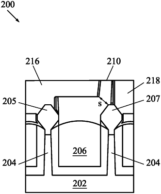
1. A semiconductor device, comprising:
a first fin and a second fin extending from a substrate, wherein a first isolation structure extends between the first fin and the second fin;
an epitaxial source/drain feature formed on the first fin;
a metal layer having a first portion over the epitaxial source/drain feature and a second portion contiguous with the first portion and extending over the first isolation structure, wherein the first portion has a thickness greater than the second portion; and
a second isolation structure over the first isolation structure, wherein the second isolation structure has a first region with an uppermost surface a first distance from a top surface of the first isolation structure and the second isolation structure has a second region having an uppermost surface a second distance from the top surface of the first isolation structure, wherein the second distance is greater than the first distance.
|