| CPC H01L 21/486 (2013.01) [H01L 21/481 (2013.01); H01L 21/4853 (2013.01); H01L 23/49827 (2013.01); H01L 25/0657 (2013.01); H01L 25/50 (2013.01); H01L 24/32 (2013.01); H01L 24/48 (2013.01); H01L 24/73 (2013.01); H01L 2224/32145 (2013.01); H01L 2224/32225 (2013.01); H01L 2224/48227 (2013.01); H01L 2224/73215 (2013.01); H01L 2224/73265 (2013.01)] | 18 Claims |
|
1. A method for forming a substrate structure for packaging, comprising:
providing a core substrate, a plurality of conductive pads at a first surface of the core substrate, and a metal layer at a second surface of the core substrate opposite to the first surface;
forming a conductive structure, for pasting the substrate structure onto an external component, on each of the plurality of conductive pads;
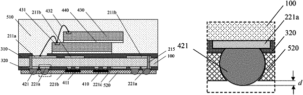
prior to forming a molding compound, attaching a semiconductor device to the first surface of the core substrate, wherein, in a direction perpendicular to and away from the first surface of the core substrate, a portion of the conductive structure exceeds a top surface of the semiconductor device;
forming the molding compound on the first surface of the core substrate to embed the semiconductor device within the molding compound and to encapsulate the conductive structure;
forming a plurality of packaging pads by patterning the metal layer at the second surface of the core substrate; and
after forming the plurality of packaging pads, removing a portion of each conductive structure at the first surface with the semiconductor device embedded within the encapsulation layer.
|