| CPC H01L 21/30655 (2013.01) [H01L 21/02603 (2013.01); H01L 21/28238 (2013.01); H01L 21/32139 (2013.01); H01L 29/0669 (2013.01); H01L 29/42372 (2013.01); H01L 29/42392 (2013.01); H01L 29/49 (2013.01); H01L 29/78391 (2014.09)] | 28 Claims |
|
1. A method for manufacturing a field-effect transistor, comprising:
forming an NMOSFET region and a PMOSFET region on a substrate, wherein the NMOSFET region and the PMOSFET region are separated by shallow trench isolation; and
forming a hard mask on the NMOSFET region and the PMOSFET region, and patterning through the hard mask; and
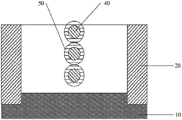
forming a multiple of stacked nanowires in the NMOSFET region and a multiple of stacked nanowires in the PMOSFET region by:
performing repeated alternating anisotropic and isotropic plasma etching in the NMOSFET region and the PMOSFET region; and
forming a passivation film by oxidizing the surface of each of the exposed nanowires by plasma after each step of etching,
wherein the passivation film has a portion located on the surface of the substrate in the NMOSFET region and the PMOSFET region and the portion is removed by anisotropic plasma to facilitate the subsequent etching; and
processing the multiple of stacked nanowires in the NMOSFET region to form a first array of nanowires in the NMOSFET region and processing the multiple of stacked nanowires in the PMOSFET region to form a second array of nanowires in the PMOSFET region; and
forming an interfacial oxide layer, a ferroelectric layer, and a stacked metal gate in sequence around each of the nanowires included in the first array and the second array.
|