| CPC G09G 3/32 (2013.01) [H05B 45/325 (2020.01); G09G 2310/0275 (2013.01)] | 25 Claims |
|
1. A method of controlling a light emitting diode (LED) device, the method comprising:
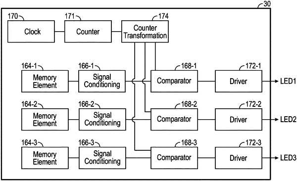
providing a plurality of LED packages, each LED package of the plurality of LED packages comprising one or more LED chips and an active electrical element with a pulse width modulation (PWM) driver;
providing a PWM signal from the PWM driver to the one or more LED chips of each LED package, the PWM signal comprising a PWM period and a PWM duty cycle that corresponds to a portion of the PWM period in which the one or more LED chips are electrically activated; and
receiving an input at the active electrical element for selecting between a numerically ordered counter sequence and a non-numerically ordered counter sequence for each PWM period of each LED package;
wherein selecting the non-numerically ordered counter sequence comprising separately segmenting the PWM duty cycle within the active electrical element of each LED package such that the one or more LED chips of each LED package are electrically activated and electrically deactivated a plurality of times within the PWM period by transforming a sequential binary counter signal into the non-numerically ordered counter sequence for the PWM period by bit reversal, wherein the bit reversal comprises reversing an order of values within a sequential binary counter value to provide a modified binary counter value of the sequential binary counter signal while maintaining a bit depth of the PWM signal.
|