| CPC G09G 3/2092 (2013.01) [G09G 2300/0426 (2013.01); G09G 2310/0278 (2013.01); G09G 2310/061 (2013.01)] | 20 Claims |
|
1. A pixel driving circuit, comprising:
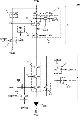
a current control sub-circuit coupled to a scan signal terminal, a gray scale data signal terminal, a first voltage signal terminal, and an enable signal terminal; the current control sub-circuit being configured to output a gray scale current signal to an element to be driven, according to a gray scale data signal from the gray scale data signal terminal, under the control of a scan signal from the scan signal terminal and an enable signal from the enable signal terminal;
a gating sub-circuit coupled to the scan signal terminal, a reset signal terminal, a gating data signal terminal, and a pulse voltage signal terminal; the gating sub-circuit being configured to drive the element to be driven to continuously emit light, under the control of the scan signal from the scan signal terminal and a gating data signal from the gating data signal terminal, and to drive the element to be driven to intermittently emit light, under the control of a reset signal from the reset signal terminal, the gating data signal from the gating data signal terminal and a pulse voltage signal from the pulse voltage signal terminal;
wherein the gating sub-circuit comprises:
a first gating unit coupled to the scan signal terminal and the gating data signal terminal; the first gating unit being configured to drive the element to be driven to continuously emit light, under the control of the scan signal from the scan signal terminal and the gating data signal from the gating data signal terminal;
a second gating unit coupled to the reset signal terminal, the gating data signal terminal, and the pulse voltage signal terminal; the second gating unit being configured to drive the element to be driven to intermittently emit light, under the control of the reset signal from the reset signal terminal, the gating data signal from the gating data signal terminal and the pulse voltage signal from the pulse voltage signal terminal; and
wherein the first gating unit comprises:
a first data writing sub-unit coupled to the scan signal terminal, the gating data signal terminal, and a first node; the first data writing sub-unit being configured to transmit the gating data signal from the gating data signal terminal to the first node under the control of the scan signal from the scan signal terminal;
a first storage sub-unit coupled to an initialization signal terminal and the first node; the first storage sub-unit being configured to store a voltage at the first node; and
a first control sub-unit coupled to the first node; the first control sub-unit being configured to drive the element to be driven to continuously emit light under the control of the voltage at the first node.
|