| CPC G06V 40/1318 (2022.01) [G06F 1/1609 (2013.01); G06F 1/1684 (2013.01)] | 20 Claims |
|
1. A display device, comprising:
a display module; and
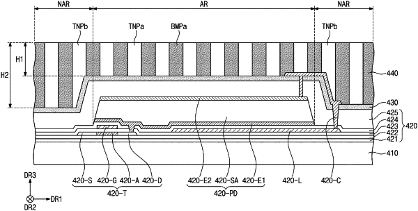
a sensor layer for detecting light reflected from a user's finger, located below the display module, and comprising:
a base layer;
a sensing layer on the base layer and comprising a sensing element for detecting the light and a transistor disposed on the base layer; and
an optical pattern layer between the sensing layer and the display module, and comprising a light-shield section defining openings arranged at intervals in a plan view, and transmission sections respectively located in the openings,
wherein the sensing element comprises:
a first sensing electrode on the base layer;
a second sensing electrode on the first sensing electrode; and
a sensing part between the first sensing electrode and the second sensing electrode, and
wherein an active region of the transistor overlaps the first sensing electrode.
|