| CPC G06T 7/0002 (2013.01) [G06N 3/045 (2023.01); G06N 3/08 (2013.01); G06T 7/337 (2017.01); G06T 2207/20024 (2013.01); G06T 2207/20081 (2013.01); G06T 2207/20084 (2013.01); G06T 2207/20224 (2013.01)] | 16 Claims |
|
1. A method, comprising:
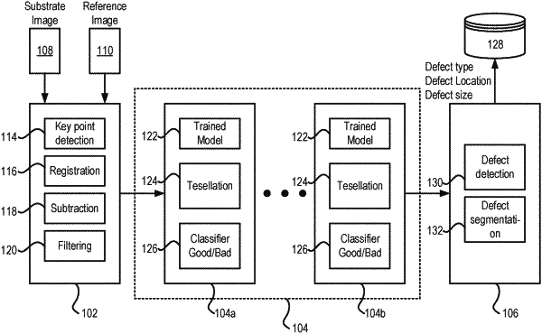
identifying a plurality of potential defect image regions in an input substrate image of an electronic substrate;
generating a plurality of image patches corresponding to the plurality of potential defect image regions, each image patch of the plurality of image patches including at least one potential defect image region of the plurality of potential defect image regions;
processing the plurality of image patches with a first defect presence classifier stage that classifies each of the plurality of image patches as containing or not containing a defect to identify, from the plurality of image patches, a set of image patches containing defect;
processing the set of image patches containing defect with a plurality of additional defect presence classifier stages, each of the plurality of additional defect presence classifier stages having at least one of a width parameter or a depth parameter that is greater than a corresponding parameter of a preceding defect presence classifier stage, each of the plurality of additional defect presence classifier stages identifying a number of image patches containing defects that is equal to or less than a number of image patches containing defects identified by a preceding defect presence classifier stage, a last defect presence classifier stage of the plurality of additional defect presence classifier stages identifying a final set of image patches containing defect;
determining a location on the electronic substrate, a size, and a type of one or more defects in the final set of image patches containing defect; and
storing in a data structure the location, the size, and the type of the one or more defects.
|