| CPC G06F 30/392 (2020.01) [H01L 27/0207 (2013.01); H01L 27/092 (2013.01)] | 20 Claims |

|
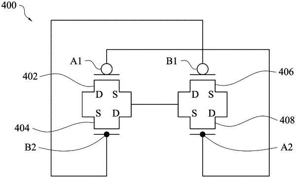
1. An integrated circuit, comprising:
a first set of conductive traces in a first level of the integrated circuit, the first set of conductive traces extending in a first direction;
a second set of conductive traces in a second level of the integrated circuit different from the first level, the second set of conductive traces extending in a second direction different from the first direction, the second set of conductive traces including:
a first conductive trace of the second set of conductive traces corresponding to a gate terminal of a first p-type transistor; and
a second conductive trace of the second set of conductive traces corresponding to a gate terminal of a first n-type transistor; and
a first conductive feature extending in the second direction, being on a third level below at least the first level;
wherein the first conductive feature corresponds to at least a first contact of a first dummy transistor;
wherein the first conductive trace of the second set of conductive traces and the second conductive trace of the second set of conductive traces are separated from each other in at least the second direction;
the first conductive trace of the second set of conductive traces is electrically coupled to the second conductive trace of the second set of conductive traces by at least the first conductive feature; and
the first n-type transistor being part of a first transmission gate; and
the first p-type transistor being part of a second transmission gate.
|