| CPC G06F 30/3323 (2020.01) [G03F 7/705 (2013.01); G03F 7/70433 (2013.01); G03F 7/70441 (2013.01); G03F 7/70508 (2013.01); G06N 5/04 (2013.01); G06F 2111/04 (2020.01); G06F 2111/10 (2020.01); G06F 2111/20 (2020.01); G06F 2119/18 (2020.01); G06N 20/00 (2019.01)] | 17 Claims |
|
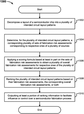
1. A method, comprising:
assigning, to a plurality of intended circuit layout patterns in a layout of a semiconductor chip, a plurality of sets of fabrication risk assessments, wherein the fabrication risk assessments in each set of fabrication risk assessments of the plurality of sets of fabrication risk assessments correspond to respective intended circuit layout patterns of the plurality of intended circuit layout patterns, the assigning comprising:
determining a first set of fabrication risk assessments based on statistical analysis of the plurality of intended circuit layout patterns; and
determining a second set of fabrication risk assessments based either on simulation of respective intended circuit layout patterns of the plurality of intended circuit layout patterns or on evaluation of empirical data for respective printed circuit layout patterns associated with respective intended circuit layout patterns of the plurality of intended circuit layout patterns;
ranking the plurality of intended circuit layout patterns based on their respective fabrication risk assessments in the plurality of sets of fabrication risk assessments; and
outputting information regarding the ranking.
|