| CPC G06F 12/10 (2013.01) [G06F 7/582 (2013.01); G06F 12/1408 (2013.01); G11C 8/12 (2013.01); G11C 11/408 (2013.01); G11C 11/4076 (2013.01); G11C 11/4096 (2013.01); G06F 2212/657 (2013.01)] | 19 Claims |
|
1. A semiconductor memory, comprising:
a memory array;
a row address processing unit, configured to output a row address;
a bank address processing unit, configured to output a bank address;
a column address processing unit, configured to output a column address; and
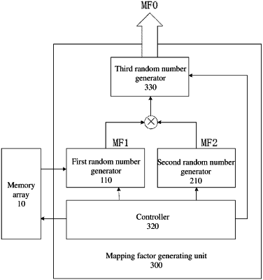
a mapping factor generating unit, configured to generate a mapping factor, wherein an output of the mapping factor generating unit is coupled to at least one of an output of the row address processing unit, an output of the bank address processing unit, and an output of the column address processing unit, and the output of the mapping factor generating unit is further coupled to the memory array,
wherein the memory array receives a result from logical processing performed on the mapping factor and at least one of the row address, the bank address, and the column address, and
wherein the mapping factor generating unit is configured so that a standard deviation of a usage rate of the at least one of the row address, the bank address and the column address is no more than 10% of an average usage rate of the at least one of the row address, the bank address and the column address.
|