| CPC G06F 3/0655 (2013.01) [G06F 3/0604 (2013.01); G06F 3/0679 (2013.01); G11C 29/025 (2013.01); G11C 29/14 (2013.01); G11C 29/18 (2013.01); G11C 29/46 (2013.01); G11C 2029/1202 (2013.01); G11C 2029/1802 (2013.01)] | 10 Claims |
|
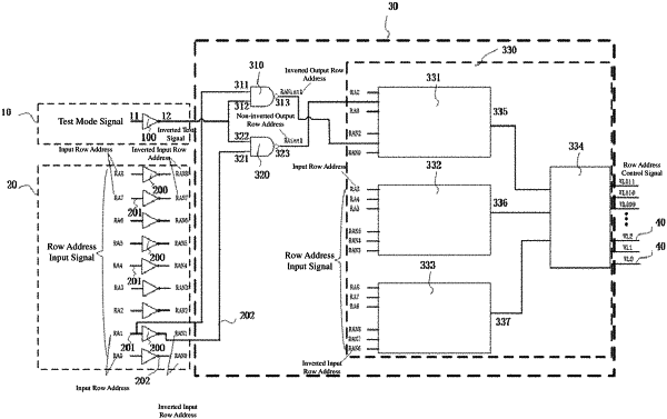
1. A word line control method for a word line control circuit device, wherein the word line control circuit device comprises a test mode input circuit, a row address input circuit, and a logic decoding processor, wherein the test mode input circuit comprises a first inverter, wherein the row address input circuit comprises a second inverter, wherein the logic decoding processor comprises a first NAND gate, a second NAND gate, and a decoding device, and wherein the word line control method comprising:
acquiring a row address input signal by the row address input circuit;
acquiring a test mode signal by the test mode input circuit;
performing logical and decoding operations on the row address input signal and the test mode signal by the logic decoding processor to generate a row address control signal, wherein the row address control signal includes at least two valid activation signals; and
simultaneously activating at least two non-adjacent word lines by the logic decoding processor based on the at least two valid activation signals,
wherein the row address input signal includes a plurality of row address signals, and wherein performing logical and decoding operations on the row address input signal and the test mode signal to generate a row address control signal comprises:
performing an inverse operation by the first inverter on the test mode signal to generate an inverted test signal;
selecting one of the plurality of row address signals, and performing a NAND operation on the selected row address signal and the inverted test signal by the first NAND gate to generate an inverted output row address;
performing inverse operations by the second inverter on all the row address signals to generate corresponding inverted row address signals;
performing a NAND operation on the inverted row address signal corresponding to the selected row address signal and the inverted test signal by the second NAND gate to generate a non-inverted output row address; and
decoding the inverted output row address, the non-inverted output row address, unselected row address signals and unselected inverted row address signals by the decoding device to obtain the row address control signal.
|