| CPC G06F 3/061 (2013.01) [G06F 3/0655 (2013.01); G06F 3/0673 (2013.01); G06F 7/5443 (2013.01); G11C 11/419 (2013.01)] | 20 Claims |
|
1. A computing device, comprising:
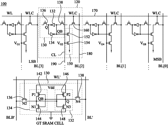
a memory array comprising a plurality of memory cells grouped in rows and columns of memory cells, each of the memory cells comprising a memory unit adapted to store data, a current source comprising a first switching device and a current generator device, and a second switching device;
a plurality of input lines, each connected to the second switching devices in a respective row and adapted to transmit an input signal to the second switching devices in the row;
a plurality of output lines, each associated with a respective column of the memory unit; and
a plurality of current controllers, each connected to the current generator devices in a respective column of the memory cells through a current control line and adapted to set a level of current generated by the current generator devices in the respective column of the memory cells, wherein the levels of currents generated by at least two of the respective current generator devices are different from each other;
wherein the second switching device in each of the columns of memory cells is adapted to connect or disconnect the current source in the memory cell to the output line associated with the column depending on the input signal received from the input line, and the first switching device in each of the memory cells is adapted to permit or prevent current flow from the current generator device depending on the data stored in the memory unit in the memory cell, and
wherein in each of the memory cells: the memory unit comprises a static random-access memory (SRAM) cell adapted to store a signal at a storage node, the first switching device comprises a first transistor having a gate connected to the storage node, the current generator device comprises a second transistor having a gate connected to the current control line associated with the column the memory cell is in, and the second switching device comprises a third transistor having a gate connected to the input line associated with the row the memory cell is in.
|