| CPC G06F 3/0412 (2013.01) [G06F 3/0443 (2019.05); H10K 50/844 (2023.02); H10K 59/122 (2023.02); H10K 59/40 (2023.02)] | 20 Claims |
|
1. A touch display panel, comprising:
a substrate comprising a display region and a non-display region, wherein the non-display region comprises a step region;
light-emitting elements disposed in the display region;
an encapsulation layer covering the light-emitting elements and at least part of the non-display region and comprising at least one inorganic layer and at least one organic layer, and wherein the at least one inorganic layer and the at least one organic layer are stacked;
a touch layer disposed on a side of the at least one inorganic layer facing away from the light-emitting elements, wherein the touch layer comprises a plurality of touch electrodes; and
a plurality of touch wires connected to the plurality of touch electrodes and extending to the non-display region along a first direction,
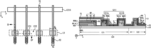
wherein the step region comprises a first region and a second region, wherein the first region is disposed adjacent the display region, wherein the second region is disposed on a side of the first region facing away from the display region, wherein the first region comprises at least one wall, wherein the second region comprises a plurality of touch terminals, and wherein at least part of the plurality of touch terminals are electrically connected to at least part of the plurality of touch wires in a one-to-one manner;
wherein the second region comprises at least one blocking column extending along a second direction, wherein the first direction and the second direction intersect, and wherein in a direction perpendicular to a plane in which the substrate is located, the at least one blocking column overlaps the plurality of touch wires extending to the non-display region;
wherein at least part of the at least one blocking column is disposed between the plurality of touch terminals and the at least one wall, and wherein the at least one blocking column is configured to prevent the at least one inorganic layer disposed between the touch layer and the substrate and in the encapsulation layer from extending to the plurality of touch terminals;
wherein the at least one blocking column comprises a plurality of sub-blocking columns, wherein in the direction perpendicular to the plane in which the substrate is located, one sub-blocking column of the plurality of sub-blocking columns overlaps one touch wire of the plurality of touch wires;
wherein a width of the one sub-blocking column in the second direction is greater than or equal to a width of one touch terminal of the plurality of touch terminals in the second direction; and
wherein
(i) one opening of at least one opening is disposed between two adjacent sub-blocking columns of the plurality of sub-blocking columns, wherein the one opening is disposed between two adjacent touch wires of the plurality of touch wires; or
(ii) the at least one blocking column comprises a blocking portion disposed between two adjacent ones of the plurality of touch wires, wherein (a) the blocking portion connects two adjacent ones of the plurality of sub-blocking columns, (b) the blocking portion comprises a first edge and a second edge opposite to each other and along the first direction, (c) at least one of the first edge or the second edge comprises an auxiliary edge structure, and (d) an edge extension direction of the auxiliary edge structure differs from the second direction.
|