| CPC G06F 1/24 (2013.01) [G06F 1/08 (2013.01); G06F 1/12 (2013.01)] | 14 Claims |
|
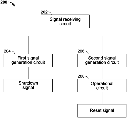
1. A system, comprising:
a signal receiving circuit that is configured to:
receive a reset configuration signal from an exceptional timing sequence device in a functional module; and
output a trigger signal;
a first signal generation circuit that is:
electrically connected to the signal receiving circuit; and
configured to generate an idle signal based at least in part on the trigger signal, wherein:
the idle signal is used to configure a shutdown signal; and
the shutdown signal is used to shut down a first clock signal of the exceptional timing sequence device and a second clock signal in a same clock domain as the first clock signal of the exceptional timing sequence device;
a second signal generation circuit that is:
electrically connected to the signal receiving circuit; and
configured to generate a reset enable signal based at least in part on the trigger signal; and
an operational circuit that is:
electrically connected to the second signal generation circuit;
configured to perform an operation based at least in part on the reset enable signal; and
configured to generate a module-based reset signal based at least in part on an operation result, wherein the module-based reset signal is used to reset the exceptional timing sequence device in the functional module.
|