| CPC G03G 15/1665 (2013.01) [G03G 15/0131 (2013.01); G03G 15/1675 (2013.01); G03G 15/5054 (2013.01); G03G 21/168 (2013.01)] | 15 Claims |
|
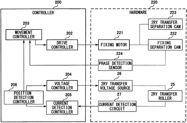
1. An image forming apparatus comprising:
an image bearing member configured to bear a toner image;
a transfer member configured to form a transfer portion where the toner image is transferred from said image bearing member onto a transfer material in contact with said image bearing member;
a moving portion configured to move said transfer member, relative to said image bearing member, to a plurality of positions including a contact position where said transfer member is contacted to said image bearing member to and a separated position where said transfer member is separated from said image bearing member;
a driving portion configured to drive said moving portion;
an applying portion configured to apply a voltage to said transfer member;
a first detecting portion configured to detect at least one of a voltage applied to said transfer member by said applying portion and a current flowing through said transfer member when the voltage is applied to said transfer member by said applying portion; and
a second detecting portion configured to detect a position of said transfer member,
wherein on the basis of a detection result of said first detecting portion acquired when a first test voltage is applied to said transfer member by said applying portion, said second detecting portion sets a second test voltage, and
wherein said second detecting portion detects the position of said transfer member on the basis of a detection result of a current value by said first detecting portion acquired when the second test voltage is applied to said transfer member by said applying portion.
|