| CPC G03F 7/7085 (2013.01) [G03F 7/70033 (2013.01); G03F 7/70916 (2013.01); G03F 7/70925 (2013.01); H05G 2/005 (2013.01); H05G 2/008 (2013.01)] | 20 Claims |
|
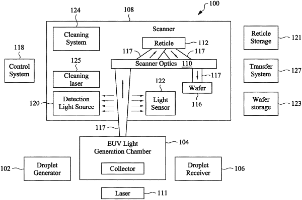
16. A photolithography system, comprising:
an extreme ultraviolet light generation chamber;
extreme ultraviolet light generation equipment configured to generate extreme ultraviolet light in the extreme ultraviolet light generation chamber; and
a scanner coupled to the extreme ultraviolet light generation chamber and configured to receive the extreme ultraviolet light from the extreme ultraviolet light generation chamber, the scanner includes:
a reticle having a pattern;
a detection light source configured to output a detection light adjacent to an aperture;
a light sensor configured to detect debris particles from the extreme ultraviolet light generation chamber by detecting interaction of the debris particles with the detection light, the extreme ultraviolet light passing between the detection light source and the light sensor; and
optical conditioning devices configured to direct the extreme ultraviolet light passed between the detection light source and the light sensor to the reticle, and direct reflected extreme ultraviolet light from the reticle to a wafer.
|