| CPC G02F 1/136295 (2021.01) [G02F 1/13452 (2013.01); H01L 23/4952 (2013.01); H01L 23/4985 (2013.01); H05K 1/189 (2013.01); H05K 2201/09736 (2013.01); H05K 2201/10681 (2013.01)] | 17 Claims |
|
1. A chip on film for a display device, the chip on film comprising:
a base substrate;
a plurality of lead wires disposed on the base substrate; and
a driving chip connected to the plurality of lead wires,
wherein each of the plurality of lead wires includes:
a first lead part having a first thickness; and
a second lead part disposed between the first lead part and the driving chip and having a second thickness greater than the first thickness, the second lead part being connected to the driving chip,
wherein the first lead part and the second lead part comprise a same material, and
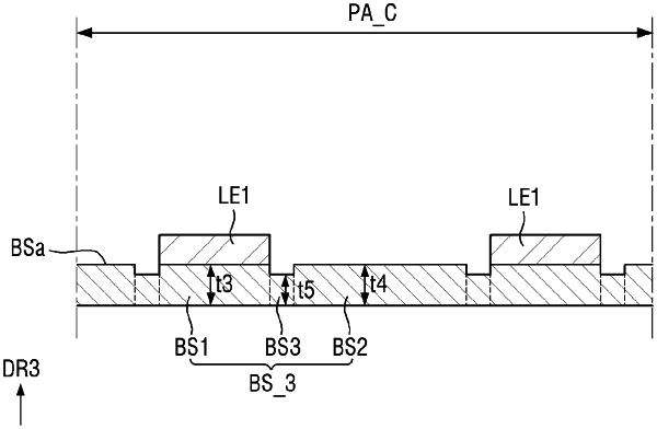
wherein the base substrate includes a first base part overlapping the first lead part, and a second base part without overlapping the first lead part,
the second base part includes a first sub-base part spaced apart from the first base part, and a second sub-base part located between the first sub-base part and the first base part, and
a thickness of the second sub-base part is smaller than each of a thickness of the first base part and a thickness of the first sub-base part.
|