|
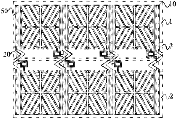
1. A color film on array (COA) substrate, comprising: a plurality of crisscrossed data lines in a first direction and scan lines in a second direction, and pixel units defined by the data lines and the scan lines; wherein the pixel units are divided into an opening region of the pixel units and a non-opening region of the pixel units; the data lines are disposed between adjacent pixel units, data line black matrix less (DBS) common electrode lines are disposed on the data lines and cover the data lines, and both the data lines and the DBS common electrode lines pass through the opening region and the non-opening region; the scan lines, transistor units, and pixel through-holes electrically connected to the transistor units are disposed in the non-opening region; each of the pixel units comprises a plurality of sub-pixel units, and each of the sub-pixel units is divided into a main-pixel region and a sub-pixel region; and each of the DBS common electrode lines bypasses the pixel through-holes in the non-opening region of the pixel units along the first direction; wherein a shape of the DBS common electrode lines in the non-opening region of the pixel units is zigzag-shaped, and an opening of a zigzag is directly defined opposite to the pixel through-holes.
|