| CPC G02F 1/136259 (2013.01) [G02F 1/133504 (2013.01); G02F 1/133516 (2013.01); G02F 1/133562 (2021.01); G02F 1/133788 (2013.01); G02F 1/133528 (2013.01)] | 10 Claims |
|
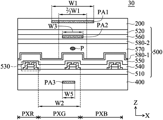
1. An electronic device, comprising:
a panel, the panel comprising:
a first substrate;
a second substrate, disposed opposite to the first substrate; and
a plurality of display units, disposed on the first substrate,
a defect, between the first substrate and the second substrate or on the second substrate; and
an optical film having a first base, a protective layer on the first base, a second base between the first base and the protective layer, and a first processed area in the second base, disposed on a top surface of the panel,
wherein in a top view of the electronic device, the first processed area corresponds to the defect, and the first processed area at least partially overlaps at least two display units, wherein a top surface of the first processed area is lower than a top surface of the second base.
|