| CPC G02F 1/134309 (2013.01) [G02F 1/1339 (2013.01); G02F 1/1368 (2013.01); G02F 1/13338 (2013.01); G02F 1/133345 (2013.01); G02F 1/136209 (2013.01); G06F 3/0412 (2013.01); G02F 1/133514 (2013.01); G02F 2202/103 (2013.01); G02F 2202/28 (2013.01); H10K 59/40 (2023.02); H10K 59/60 (2023.02)] | 16 Claims |
|
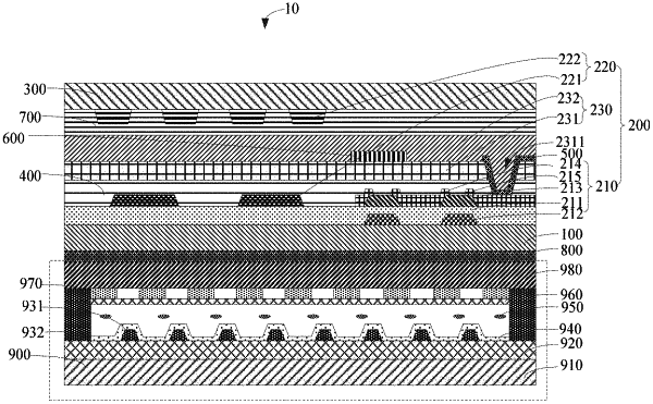
1. A display device, comprising:
a first substrate;
a first array structure layer disposed on the first substrate, wherein the first array structure layer comprises a photosensitive sensor, a touch sensor, and a spacer layer, the photosensitive sensor comprises a gate, a semiconductor portion, a source, and a drain, the touch sensor comprises a transmitting electrode and a receiving electrode, the spacer layer is disposed between the photosensitive sensor and the receiving electrode, and the receiving electrode is disposed on a side of the spacer layer away from the photosensitive sensor; and
a second substrate disposed on the first array structure layer,
wherein the spacer layer comprises a first spacer sub-layer, and the first spacer sub-layer is disposed between the photosensitive sensor and the receiving electrode, and
wherein the display device further comprises a light shielding layer disposed on the first spacer sub-layer and disposed on the semiconductor portion.
|