| CPC G02F 1/133609 (2013.01) [G02F 1/133512 (2013.01); G02F 1/133514 (2013.01); G02F 1/133553 (2013.01); G02F 1/133603 (2013.01); G02F 1/133621 (2013.01); G06F 3/0412 (2013.01); G06F 3/0481 (2013.01); G06F 21/32 (2013.01); H01L 25/0753 (2013.01); H01L 33/44 (2013.01); H10K 59/50 (2023.02); G02F 1/133614 (2021.01); G02F 1/133617 (2013.01); G02F 2202/36 (2013.01); G06F 2221/2133 (2013.01)] | 9 Claims |
|
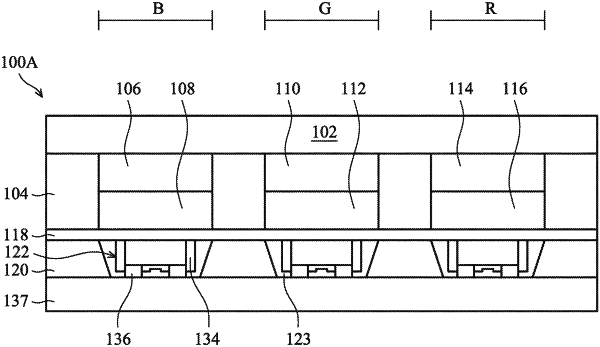
1. A display device, comprising:
a substrate;
a plurality of pixels disposed on the substrate, wherein one of the plurality of pixels comprises a first light filter layer;
a first light shielding layer defining a plurality of openings, wherein the first light filter layer is disposed in one of the plurality of openings;
a second light shielding layer disposed on the substrate and at least partially overlapped with the first light shielding layer, and the second light shielding layer defining a plurality of another openings;
a plurality of light emitting diodes disposed in the another plurality of another openings; and
a material layer disposed between the first light shielding layer and the second light shielding layer,
wherein in a direction parallel to an upper surface of the substrate, the second light shielding layer overlaps the plurality of light emitting diodes,
wherein the material layer overlaps with at least two of the plurality of light emitting diodes, and the material layer comprises silicon oxide material or oxygen-containing material.
|