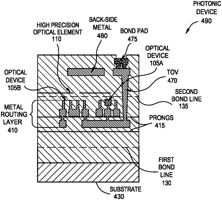
| CPC G02B 6/43 (2013.01) [G02B 6/425 (2013.01); G02B 6/4236 (2013.01); G02B 6/4274 (2013.01); G02B 6/4204 (2013.01)] | 19 Claims |

|
1. A method, comprising:
providing an optical device in a first semiconductor wafer;
providing an optical element in a second semiconductor wafer;
wafer bonding the first semiconductor wafer and the second semiconductor wafer to form a combined wafer, wherein bonding the first semiconductor wafer and the second semiconductor wafer optically couples the optical device to the optical element, and wherein the optical device is optically coupled to the optical element to form an optical adapter for transmitting an optical signal between the optical device and an external light source;
removing a substrate corresponding to the second semiconductor wafer from the combined wafer; and
performing a second wafer bonding process either (i) before forming the combined wafer or (ii) after removing the substrate corresponding to the second semiconductor wafer.
|