| CPC G02B 6/356 (2013.01) [G02B 6/1225 (2013.01)] | 2 Claims |
|
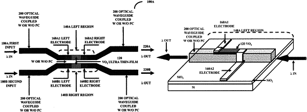
1. An optical switch comprising:
a first optical waveguide and a second optical waveguide,
wherein the first optical waveguide is less than 5 microns in horizontal width, wherein the second optical waveguide is less than 5 microns in horizontal width,
wherein a section of the first optical waveguide is substantially parallel within manufacturing tolerance to a section of the second optical waveguide,
wherein the section of the first optical waveguide is optically coupled with an ultra thin-film of a vertical thickness or a vertical depth less than 0.5 microns,
wherein the ultra thin-film comprises: a phase transition material,
wherein the phase transition material on the first optical waveguide is receiving a first stimulant, just to induce insulator-to-metal (IMT) phase transition in the phase transition material on the first optical waveguide,
wherein the said insulator-to-metal (IMT) phase transition is with a change in lattice structure or without a change in lattice structure, and/or,
wherein the section of the second optical waveguide is optically coupled with the ultra thin-film of a vertical thickness or a vertical depth less than 0.5 microns,
wherein the ultra thin-film comprises: the phase transition material,
wherein the phase transition material on the second optical waveguide is receiving a second stimulant, just to induce insulator-to-metal (IMT) phase transition in the phase transition material on the second optical waveguide, and
wherein the said insulator-to-metal (IMT) phase transition is with a change in lattice structure or without a change in lattice structure; and
wherein the optical switch is flip-chip mounted on a nanoscaled fin array and/or a heat dissipating substrate, wherein the nanoscaled fin array comprises an array of nanoscaled metal pillars embedded in a thermally conducting thin-film.
|