| CPC G01R 31/318583 (2013.01) [G01R 31/31723 (2013.01); G01R 31/31924 (2013.01); G01R 31/318541 (2013.01); G01R 31/318572 (2013.01); H03K 3/02332 (2013.01); H03K 3/0372 (2013.01); H03K 3/35625 (2013.01)] | 15 Claims |
|
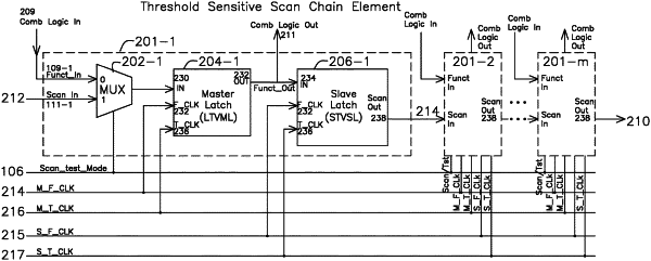
1. A scan chain element comprising:
a functional logic input and a functional logic output;
a multiplexer selecting between the functional logic output and a test input according to a Scan_test_Mode input, the multiplexer coupling a selection to a mux output;
a low threshold voltage master latch (LTVML) having an input coupled to the mux output, the LTVML generating an output coupled to the functional logic input;
a standard threshold voltage slave latch (STVSL) having an input coupled to the LTVML output and configured to provide a test output for a subsequent scan chain element;
a master functional clock (M_F_CLK) input and master test clock (M_T_CLK) input coupled to the LTVML, the LTVML latching the mux output when the M_T_CLK is 1 and the M_F_CLK is 0;
a slave functional clock (S_F_CLK) input and a slave test clock (S_T_CLK) input coupled to the STVSL, the STVSL latching the LTVML output when the S_T_CLK is 1 and the S_F_CLK is 0;
where the S_T_CLK and S_F_CLK are not active when the multiplexer selects the functional logic output, and the S_T_CLK is 180 degrees out of phase from the S_F_CLK when the Scan_test_Mode input asserts a test mode.
|