| CPC G01R 31/2891 (2013.01) [G01R 31/2887 (2013.01); H01L 22/12 (2013.01)] | 5 Claims |
|
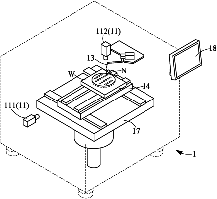
1. A semiconductor inspecting method, comprising multiple steps of:
(a) defining a first position of a probe needle in a image from above by adopting a vision system of a semiconductor inspecting system;
(b) making a first relative vertical movement between the probe needle and the pad by adopting a driving system of the semiconductor inspecting system;
(c) recognizing whether the probe needle corresponding to the first position in the image has a minimum change in position due to the first relative vertical movement by adopting the vision system of the semiconductor inspecting system; and
(d) once the minimum change in position of the probe needle caused by the probe needle being contacted with the pads is recognized, stopping the first relative vertical movement by adopting the driving system of the semiconductor inspecting system;
wherein the step (c) further comprises multiple steps of:
(c1) obtaining a second position of the probe needle in the image by adopting the vision system; and
(c2) comparing the second position with the first position to recognize whether the probe needle is contacted with the pad or not;
wherein the second position is defined as a position of the probe needle on the pad in the image after the first relative vertical movement and the probe needle being contacted with the pad to generate the minimum change in position of the probe needle.
|