| CPC G01R 31/2849 (2013.01) [G01R 1/07342 (2013.01)] | 12 Claims |
|
1. A cryogenic wafer test system comprising:
a first chamber that is cooled to a cryogenic temperature;
a wafer chuck confined within the first chamber, the wafer chuck being configured to accommodate a wafer device-under-test (DUT) comprising a plurality of superconducting die;
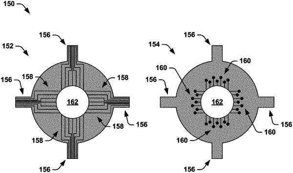
a probe card configured to implement a test on a superconducting die of the plurality of superconducting die via a plurality of electrical probe contacts, the probe card including at least one through-hole that extends from a first surface to an opposite second surface to facilitate alignment of a plurality of electrical contacts on a surface of the superconducting die to a respective plurality of electrical probe contacts on the opposing second surface of the probe card, the probe card including a plurality of electrical lines that extend from the first surface through the at lease one through-hole and connect to the respective plurality of electrical probe contacts on the second surface of the probe card; and
a wafer chuck actuator system confined within a second chamber, the wafer chuck actuator system being configured to provide at least one of translational and rotational motion of the wafer chuck to facilitate alignment and contact of the plurality of electrical contacts of the superconducting die to the respective plurality of electrical probe contacts of the probe card.
|