| CPC G01R 31/26 (2013.01) [G01R 31/2886 (2013.01); G01R 31/308 (2013.01)] | 16 Claims |
|
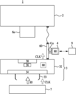
1. An image test system, comprising:
a test assembly for obtaining a test signal from a test object, wherein the test assembly comprises an interface conversion circuit for converting signal transmission form of the test signal; and
an image capture card for obtaining the test signal from the test assembly, and obtaining an image data from the test signal,
wherein the image test system further comprises a test signal clock generation circuit for obtaining a test signal clock from the test signal,
wherein the test signal comprises a first sub-signal, a second sub-signal and a third sub-signal, and the test signal clock generation circuit comprises a first input terminal, a first clock obtaining module, a second input terminal, a second clock obtaining module, a third input terminal, a third clock obtaining module and a circuit output terminal, and wherein the first input terminal is provided for obtaining the first sub-signal, the first clock obtaining module is provided for obtaining a first sub-signal clock from the first sub-signal and transmitting the first sub-signal clock to the circuit output terminal, the second input terminal is provided for obtaining the second sub-signal, the second clock obtaining module is provided for obtaining a second sub-signal clock from the second sub-signal and transmitting the second sub-signal clock to the circuit output terminal, the third input terminal is provided for obtaining the third sub-signal, the third clock obtaining module is provided for obtaining a third sub-signal clock from the third sub-signal and transmitting the third sub-signal clock to the circuit output terminal, and the circuit output terminal is provided for combining the first sub-signal clock, the second sub-signal clock and the third sub-signal clock to form the test signal clock.
|