| CPC G01R 1/0433 (2013.01) [H01R 12/7076 (2013.01)] | 20 Claims |
|
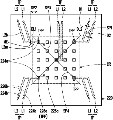
1. A testing apparatus for a semiconductor package, comprising:
a circuit board, having a testing region and comprising a plurality of testing contacts and a plurality of signal contacts distributed in the testing region;
testing patterns, embedded in the circuit board and electrically connected to the testing contacts, wherein each of the testing patterns comprises:
a first conductive line; and
a second conductive line, comprising a main portion and a branch portion connected to main portion, wherein the first conductive line is connected to the main portion; and
a socket, located on the circuit board and comprising connectors electrically connected to the circuit board, wherein the connectors are configured to transmit electric signals for testing the semiconductor package from the testing apparatus.
|