| CPC H01L 39/2493 (2013.01) [H01L 29/06 (2013.01)] | 20 Claims |
|
1. A topological quantum computing device comprising:
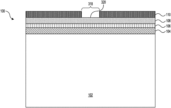
a quantum well formed in a substrate;
a superconducting metal layer formed on a surface of the substrate; and
a gate dielectric formed over the superconducting metal layer after selectively removing a portion of the superconducting metal layer to define a topologically active area of the topological quantum computing device, wherein the gate dielectric is formed after subjecting the substrate to a plasma treatment, wherein a set of parameters associated with the plasma treatment is selected to both increase channel mobility of a channel adjacent to the quantum well associated with the topological quantum computing device and increase a density of electrons within the quantum well, and wherein the plasma treatment further results in a formation of a clean semiconductor-dielectric interface between the topologically active area of the topological quantum computing device and a topologically inactive area of the topological quantum computing device.
|