| CPC H10K 59/126 (2023.02) [H10K 59/1213 (2023.02); H10K 59/1216 (2023.02); H10K 59/131 (2023.02)] | 20 Claims |
|
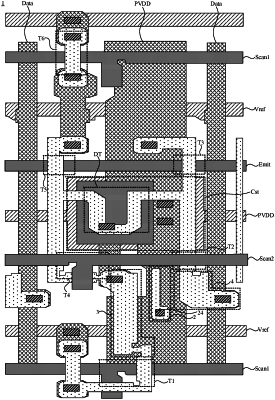
1. A display panel, comprising:
a plurality of pixel circuits arranged in a matrix; and
a blocking unit,
wherein each of the plurality of pixel circuits comprises:
a driving transistor having a gate electrode and a first electrode;
a first switch transistor having a gate electrode electrically connected to a first scanning signal line, a first electrode electrically connected to a reference voltage signal line, and a second electrode electrically connected to the gate electrode of the driving transistor;
a second switch transistor, having a gate electrode electrically connected to a second scanning signal line, a first electrode electrically connected to a data line, and a second electrode electrically connected to the first electrode of the driving transistor; and
a third switch transistor having a gate electrode electrically connected to a light-emitting control signal line, a first electrode electrically connected to a power supply voltage signal line, and a second electrode electrically connected to the first electrode of the driving transistor;
wherein the blocking unit is configured to directly receive a fixed potential signal, and at least a partial area of the blocking unit is located between a first semiconductor connection portion and a second semiconductor connection portion that is mechanically disconnected from the blocking unit, the first semiconductor connection portion is a semiconductor electrically connected between the second electrode of the first switch transistor and the gate electrode of the driving transistor, and the second semiconductor connection portion is a semiconductor electrically connected between the first electrode of the second switch transistor and the data line;
wherein the first semiconductor connection portion and the second semiconductor connection portion are arranged along a straight line parallel to the second scanning signal line, and at least a part of the blocking unit is located between the first semiconductor connection portion and the second semiconductor connection portion along the straight line;
wherein the blocking unit comprises a second blocking unit, wherein the second blocking unit is disposed between the first semiconductor connection portion of one pixel circuit of the plurality of pixel circuits and the second semiconductor connection portion of another pixel circuit of the plurality of pixel circuits that is adjacent to the one pixel circuit in a first direction, the first direction intersecting with a second direction and the second direction being an extension direction of the data line; and
wherein the second blocking unit, the first semiconductor connection portion and the second semiconductor connection portion each have an upper edge and a lower edge that extend in the first direction, the upper edge being close to the second scanning signal line and the lower edge being close to the reference voltage signal line; and
wherein an extension line of the lower edge of the second blocking unit is located between the lower edge of the second semiconductor connection portion and the reference voltage signal line.
|