US 11,690,257 B2
Display device and manufacturing method thereof
Jae Sik Kim, Hwaseong-si (KR); Woo Yong Sung, Seoul (KR); and Byoung Kwon Choo, Hwaseong-si (KR)
Assigned to SAMSUNG DISPLAY CO., LTD., Gyeonggi-Do (KR)
Filed by Samsung Display Co., LTD., Yongin-si (KR)
Filed on Sep. 5, 2022, as Appl. No. 17/903,003.
Application 17/903,003 is a division of application No. 17/019,445, filed on Sep. 14, 2020, granted, now 11,437,450.
Claims priority of application No. 10-2020-0031526 (KR), filed on Mar. 13, 2020.
Prior Publication US 2022/0415985 A1, Dec. 29, 2022
Int. Cl. H01L 27/32 (2006.01); H10K 59/123 (2023.01); H10K 71/00 (2023.01); H10K 71/20 (2023.01); H10K 59/12 (2023.01); H10K 102/00 (2023.01); H10K 102/10 (2023.01)
CPC H10K 59/123 (2023.02) [H10K 71/00 (2023.02); H10K 71/20 (2023.02); H10K 59/1201 (2023.02); H10K 2102/00 (2023.02); H10K 2102/103 (2023.02)] 12 Claims
OG exemplary drawing
 
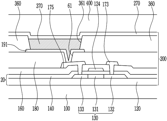
1. A display device comprising:
a substrate;
an inorganic insulating layer disposed on the substrate;
a conductor disposed on the inorganic insulating layer; and
an organic insulating layer disposed on the conductor, wherein an opening is defined through the organic insulating layer to exposes a part of an upper surface of the conductor, and
at least one material selected from a siloxane, a thiol, a phosphate, a disulfide including a sulfur series, and an amine is bonded on the part of the upper surface of the conductor exposed through the opening.