| CPC H10K 59/122 (2023.02) [H10K 50/84 (2023.02); H10K 50/844 (2023.02); H10K 71/00 (2023.02); H10K 59/1201 (2023.02)] | 30 Claims |
|
1. A method of forming a device, comprising:
positioning a substrate having:
an anode,
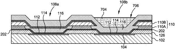
a first opening of a first sub-pixel defined by adjacent first inorganic overhang structures disposed over adjacent pixel-defining layer (PDL) structures disposed over the substrate;
depositing, at an OLED angle θOLED defined using the first inorganic overhang structures, a first OLED material over a first portion and a second portion of the substrate, the first portion corresponding to the first sub-pixel and the second portion corresponding to a second sub-pixel;
depositing, at a cathode angle θcathode defined using the first inorganic overhang structures, a first cathode over the first portion and the second portion of the substrate, wherein the first inorganic overhang structures are used in defining deposition angles of the OLED angle θOLED and the cathode angle θcathode;
depositing a first encapsulation layer over the first cathode and over the first portion and the second portion of the substrate such that the first sub-pixel comprises:
the first OLED material having an OLED edge extending under first and second extensions of an upper portion of the first inorganic overhang structures; and
the first cathode extending under the first and second extensions of the upper portion of the first inorganic overhang structures and past the OLED edge; and
removing the first OLED material, the first cathode, and the first encapsulation layer over the second portion.
|