| CPC H10K 59/121 (2023.02) [G02F 1/1368 (2013.01); G02F 1/13629 (2021.01); H04N 23/45 (2023.01); H04N 23/57 (2023.01); H10K 59/131 (2023.02)] | 20 Claims |
|
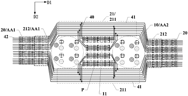
1. A display panel, comprising:
a display region and a non-display region, wherein:
the display region includes a first display region and at least one second display region;
the first display region at least partially surrounds the at least one second display region;
each second display region of the at least one second display region includes at least two photosensitive device setting regions and a spacing region disposed between the at least two adjacent photosensitive device setting regions;
the display region is provided with a plurality of sub-pixels and pixel driving circuits electrically connected to the plurality of sub-pixels;
the pixel driving circuits corresponding to the plurality of sub-pixels in the spacing region are electrically connected to the pixel driving circuits located in the first display region through signal lead wires; and
the signal lead wires are arranged on both sides of sub-pixel rows along a first direction.
|