| CPC H10K 50/844 (2023.02) [H10K 59/122 (2023.02); H10K 59/40 (2023.02); H10K 59/65 (2023.02); G09G 2300/0408 (2013.01); G09G 2300/0804 (2013.01); H01L 27/14678 (2013.01); H10K 50/818 (2023.02); H10K 50/856 (2023.02); H10K 59/1216 (2023.02); H10K 59/35 (2023.02); H10K 2102/00 (2023.02)] | 26 Claims |
|
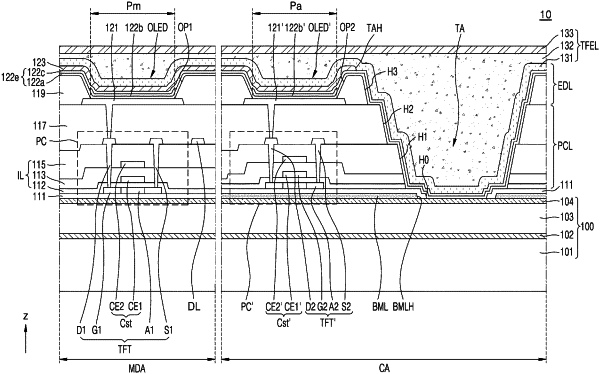
1. A display panel including a main display area, a component area including a transmission area, and a peripheral area outside the main display area, the display panel comprising:
a substrate;
an inorganic insulating layer over the substrate and including a first hole corresponding to the transmission area;
a planarization layer over the inorganic insulating layer;
a pixel definition layer over the planarization layer and having a thickness of 1.3 μm to 2 μm; and
a thin film encapsulation layer over the pixel definition layer,
wherein an angle between a side surface of the pixel definition layer and an upper surface of the planarization layer is 30 degrees to 40 degrees.
|