| CPC H01L 51/5278 (2013.01) [C09K 11/883 (2013.01); H01L 51/0072 (2013.01); H01L 51/502 (2013.01)] | 25 Claims |
|
1. A light emitting device, comprising
a first electrode and a second electrode facing each other;
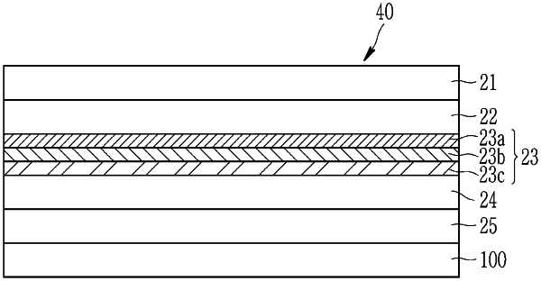
an emissive layer disposed between the first electrode and the second electrode;
wherein the emissive layer comprises a layer comprising:
an organic compound having a bipolar transport property, and
a plurality of quantum dots that are configured to emit light of a predetermined color, wherein the emissive layer further comprises a halogen, a p-type semiconductor material, and n-type semiconductor material, or a combination thereof, and
wherein a thickness of the emissive layer is greater than or equal to about 30 nm and less than or equal to about 200 nm.
|