| CPC H10K 50/16 (2023.02) [H10K 50/15 (2023.02); H10K 50/171 (2023.02); H10K 50/865 (2023.02); H10K 59/122 (2023.02); H10K 71/00 (2023.02)] | 20 Claims |
|
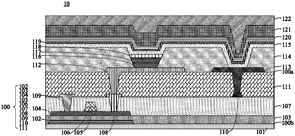
1. A display panel, comprising:
a driving circuit layer comprising a first surface and a second surface disposed opposite to each other;
a first electrode layer partially covering the first surface;
an auxiliary electrode layer partially covering the first surface, wherein the auxiliary electrode layer and the first electrode layer are disposed at a same level, and a gap is defined between the auxiliary electrode layer and the first electrode layer;
a pixel definition layer covering the driving circuit layer, the first electrode layer, and the auxiliary electrode layer, wherein a first via hole is defined on the pixel definition layer; and
an electron transport layer disposed on a side of the pixel definition layer away from the driving circuit layer and connected to the auxiliary electrode layer through the first via hole;
wherein an energy level difference between a lowest unoccupied molecular orbital of the electron transport layer and a work function of the auxiliary electrode layer is 2.0 eV or less.
|