| CPC H10B 61/00 (2023.02) [H01L 23/5226 (2013.01); H01L 23/5283 (2013.01); H10N 50/01 (2023.02); H10N 50/80 (2023.02)] | 18 Claims |
|
1. A non-volatile memory device, comprising:
a substrate, having a memory region and a dummy region surrounding the memory region;
an interconnect structure, disposed on the substrate and located in the memory region;
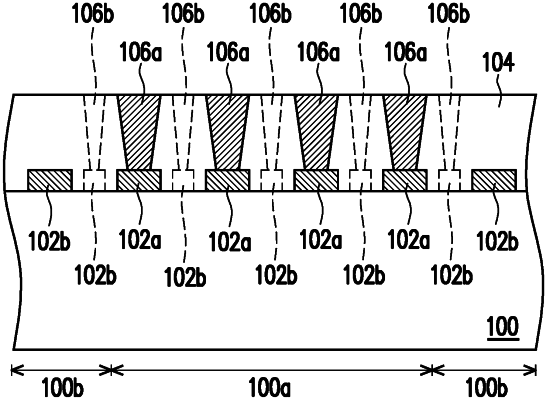
a plurality of memory cells, disposed on the interconnect structure and arranged in an array when viewed from a top view, wherein the plurality of memory cells comprises a plurality of first memory cells located in the memory region and a plurality of second memory cells located in the dummy region;
a plurality of conductive vias, disposed in the memory region and located between the plurality of first memory cells and the interconnect structure to electrically connect each of the first memory cells and the interconnect structure, respectively; and
a plurality of dummy vias, disposed in the dummy region and surrounding the memory region,
wherein the aperture of the dummy vias is smaller than the aperture of the conductive vias.
|