US 11,690,229 B2
Magnetoresistive stack with seed region and method of manufacturing the same
Jijun Sun, Chandler, AZ (US); Sanjeev Aggarwal, Scottsdale, AZ (US); Han-Jong Chia, Hsinchu (TW); Jon M. Slaughter, Slingerlands, NY (US); and Renu Whig, Chandler, AZ (US)
Assigned to EVERSPIN TECHNOLOGIES, INC., Chandler, AZ (US)
Filed by Everspin Technologies, Inc., Chandler, AZ (US)
Filed on Dec. 23, 2020, as Appl. No. 17/131,926.
Application 17/131,926 is a continuation of application No. 16/870,099, filed on May 8, 2020, granted, now 10,910,434.
Application 16/870,099 is a continuation of application No. 16/601,848, filed on Oct. 15, 2019, granted, now 10,692,926, issued on Jun. 23, 2020.
Application 16/601,848 is a continuation of application No. 16/195,178, filed on Nov. 19, 2018, granted, now 10,483,320, issued on Nov. 19, 2019.
Application 16/195,178 is a continuation in part of application No. 15/373,880, filed on Dec. 9, 2016, granted, now 10,141,498, issued on Nov. 27, 2018.
Claims priority of provisional application 62/712,578, filed on Jul. 31, 2018.
Claims priority of provisional application 62/265,650, filed on Dec. 10, 2015.
Prior Publication US 2021/0111223 A1, Apr. 15, 2021
Int. Cl. H01L 27/22 (2006.01); H01L 43/02 (2006.01); H01L 43/08 (2006.01); G11C 11/16 (2006.01); H01L 43/12 (2006.01); G11B 5/39 (2006.01); H01L 43/10 (2006.01)
CPC H01L 27/222 (2013.01) [G11B 5/3909 (2013.01); G11C 11/1673 (2013.01); H01L 43/02 (2013.01); H01L 43/08 (2013.01); H01L 43/10 (2013.01); H01L 43/12 (2013.01)] 20 Claims
OG exemplary drawing
 
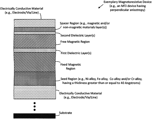
1. A magnetoresistive stack comprising:
an electrically conductive material;
a seed region disposed above the electrically conductive material, wherein the seed region includes tantalum;
a fixed magnetic region disposed above the seed region, wherein the fixed magnetic region includes a synthetic antiferromagnetic structure comprising:
a first ferromagnetic region disposed above the seed region;
a coupling layer disposed on and in contact with the first ferromagnetic region; and
a second ferromagnetic region disposed on and in contact with the coupling layer;
a first dielectric layer disposed above the second ferromagnetic region;
a free magnetic region disposed above the first dielectric layer;
a second dielectric layer disposed above the free magnetic region; and
a third magnetic region disposed above the second dielectric layer.