| CPC H10B 51/30 (2023.02) [H01L 21/76876 (2013.01); H10B 53/30 (2023.02)] | 20 Claims |
|
1. A method comprising:
forming a first conductive layer over a substrate;
forming a seed layer over the first conductive layer, wherein the seed layer comprises a crystal structure comprising multiple phases, and wherein a first value is equal to a percent of the crystal structure of the seed layer in an orthorhombic phase;
performing an annealing process to form an annealed seed layer, wherein the annealed seed layer comprises a crystal structure comprising multiple phases, and wherein a second value is equal to a percent of the annealed seed layer in the orthorhombic phase, and wherein the second value is greater than the first value;
forming a memory layer over the annealed seed layer; and
forming a second conductive structure over the memory layer;
wherein a thickness of the seed layer before the annealing process is a same as a thickness of the annealed seed layer upon completion of the annealing process.
|
|
7. A method comprising:
forming a gate electrode over a substrate;
forming a seed layer over the gate electrode;
performing an annealing process to form an annealed seed layer;
forming a memory layer over the annealed seed layer;
forming an active layer over the memory layer; and
forming a source contact and a drain contact over the active layer;
wherein the forming of the seed layer comprises:
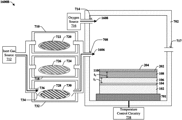
flowing an inert gas over a solid precursor comprising a metal to generate a precursor vapor comprising the metal; and
flowing the precursor vapor and oxygen gas over the gate electrode to deposit the seed layer on the gate electrode; and
wherein a thickness of the seed layer before the annealing process is a same as a thickness of the annealed seed layer upon completion of the annealing process.
|
|
14. A method comprising:
forming a conductive layer overlying a substrate;
forming a crystalline seed layer overlying the conductive layer;
annealing the crystalline seed layer, wherein an orthorhombic phase increases in the crystalline seed layer from a beginning of the annealing to an end of the annealing;
depositing a ferroelectric layer overlying and directly on the crystalline seed layer;
depositing a semiconductor layer overlying the ferroelectric layer; and
forming a source electrode and a drain electrode overlying the semiconductor layer;
wherein the forming of the crystalline seed layer and the annealing are performed within a common process chamber.
|