| CPC H10B 43/40 (2023.02) [H01L 21/26513 (2013.01); H01L 21/28052 (2013.01); H01L 21/28518 (2013.01); H01L 29/40114 (2019.08); H01L 29/40117 (2019.08); H01L 29/42328 (2013.01); H01L 29/42344 (2013.01); H01L 29/456 (2013.01); H01L 29/4933 (2013.01); H01L 29/6659 (2013.01); H01L 29/66545 (2013.01); H01L 29/66833 (2013.01); H01L 29/7833 (2013.01); H01L 29/792 (2013.01); H10B 41/30 (2023.02); H10B 41/49 (2023.02); H10B 43/30 (2023.02); H10B 43/35 (2023.02); H01L 29/517 (2013.01)] | 21 Claims |
|
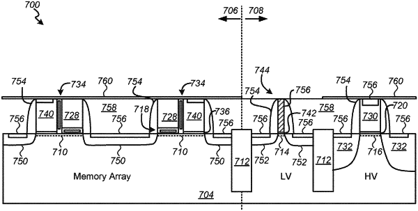
1. A method of fabricating a semiconductor device comprising:
forming a charge trapping stack over a surface of a substrate in a memory region;
forming a gate dielectric over the surface of the substrate in a peripheral region;
depositing a first polysilicon layer and a height-enhancing (HE) film over the surface of the substrate in the memory region and the peripheral region;
patterning the HE film, first polysilicon layer, and the charge trapping stack to form a memory-gate in the memory region;
patterning the HE film, first polysilicon layer, and the gate dielectric in a high voltage (HV) area in the peripheral region to form a HV-gate;
depositing a second polysilicon layer over the surface of the substrate;
planarizing the second polysilicon layer to remove portions of the second polysilicon layer extending above the memory-gate and HV-gate; and
implanting ions to form a first source/drain (S/D) region in the substrate adjacent to the HV-gate, wherein the first S/D region comprises the ions implanted to a depth in the substrate greater than a height of the HV-gate above the surface of the substrate.
|