| CPC H10B 12/34 (2023.02) [H10B 12/03 (2023.02); H10B 12/36 (2023.02); H10B 12/482 (2023.02); H10B 12/485 (2023.02); H10B 12/488 (2023.02)] | 20 Claims |
|
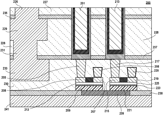
15. A DRAM memory cell structure, comprising:
a bottom gate;
a dielectric formed above the bottom gate;
channel material formed above the dielectric comprising a first portion that is parallel to the gate and second and third portions that are orthogonal to the gate;
a capacitor landing structure coupled to the second portion of the channel material; and
a bitline coupled to the third portion of the channel material wherein the capacitor landing structure is extends above the bitline, and wherein the capacitor landing structure has a bottommost surface at a same level as a bottommost surface of the bitline.
|