| CPC H10B 10/12 (2023.02) [H10B 10/18 (2023.02)] | 20 Claims |
|
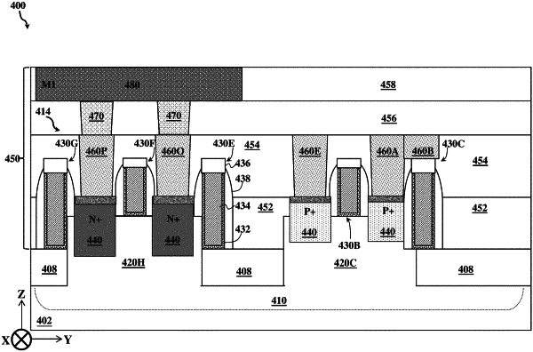
1. An integrated circuit device comprising:
a first FinFET disposed over a doped region of a first type dopant, wherein the first FinFET includes a first fin structure and first source/drain (S/D) features, the first fin structure having a first width;
a second FinFET disposed over the doped region, wherein the second FinFET includes a second fin structure and second source/drain (S/D) features, the second fin structure having a second width;
a fin-based well strap disposed over the doped region, wherein the fin-based well strap includes a third fin structure and third S/D features, the third fin structure having a third width that is larger than either of the first width or the second width, wherein the fin-based well strap is configured to bias the doped region to a bias voltage;
a first fin stub connecting a bottom portion of the first fin structure with a bottom portion of the third fin structure; and
a second fin stub connecting a bottom portion of the second fin structure with the bottom portion of the third fin structure.
|