| CPC H05K 1/147 (2013.01) [H01L 25/18 (2013.01); H05K 1/189 (2013.01); H05K 1/0346 (2013.01); H05K 1/09 (2013.01); H05K 2201/0154 (2013.01); H05K 2201/049 (2013.01); H05K 2201/058 (2013.01); H05K 2201/10128 (2013.01); H05K 2201/10136 (2013.01)] | 19 Claims |
|
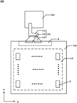
1. A connection structure configured to connect a display panel and a circuit board, the connection structure comprising:
a flexible printed circuit; and
a first chip-on-film and a second chip-on-film that are coupled to one end of the flexible printed circuit, wherein
the first chip-on-film and the second chip-on-film are coupled to two surfaces of the flexible printed circuit that are opposite in a thickness direction of the flexible printed circuit;
wherein the first chip-on-film includes a first portion disposed on and in direct contact with the flexible printed circuit, the second chip-on-film includes a second portion disposed on and in direct contact with the flexible printed circuit and an orthogonal projection of the first portion on a plane perpendicular to the thickness direction of the flexible printed circuit and an orthogonal projection of the second portion on the plane at least partially overlap.
|