| CPC H05K 1/118 (2013.01) [G06F 3/0412 (2013.01); G06F 3/0443 (2019.05); G06F 3/0446 (2019.05); H01R 12/61 (2013.01); H05K 3/363 (2013.01); G06F 3/04164 (2019.05); H05K 1/189 (2013.01); H05K 2201/041 (2013.01); H05K 2201/0939 (2013.01); H05K 2201/09227 (2013.01); H05K 2201/09236 (2013.01); H05K 2201/09381 (2013.01); H05K 2201/09481 (2013.01); H05K 2201/10128 (2013.01); H10K 59/131 (2023.02); H10K 59/179 (2023.02)] | 42 Claims |

|
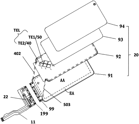
1. A display device, comprising:
a display panel comprising:
a display area, wherein a plurality of sub-pixels provided in an array, and a plurality of scanning lines and a plurality of data lines intersecting each other are provided in the display area, the plurality of scanning lines extend along a first direction and the plurality of data lines extend along a second direction different from the first direction; and
a peripheral area surrounding the display area, wherein a plurality of first connection terminals, a plurality of second connection terminals, a plurality of third connection terminals, a plurality of fourth connection terminals, a plurality of fifth connection terminals and a driving control circuit are provided in the peripheral area on a first side of the display panel, the plurality of data lines are respectively electrically connected with the plurality of first connection terminals, the plurality of first connection terminals are spaced from the plurality of second connection terminals, the driving control circuit is electrically connected with the plurality of first connection terminals and the plurality of second connection terminals, the fifth connection terminals are respectively electrically connected with the second connection terminals through connection wires, a total number of the plurality of first connection terminals is larger than that of the plurality of fifth connection terminals, and the plurality of fifth connection terminals are closer to an edge of the first side of the display panel than the plurality of first connection terminals and the plurality of second connection terminals;
a flexible circuit board, electrically connected with the display panel, wherein a side of the flexible circuit board is provided with a plurality of first wiring terminals, a plurality of second wiring terminals and a plurality of third wiring terminals, the plurality of first wiring terminals are respectively electrically connected with the plurality of third connection terminals, the plurality of second wiring terminals are respectively electrically connected with the plurality of fourth connection terminals, the plurality of third wiring terminals are respectively electrically connected with the plurality of fifth connection terminals, and the flexible circuit board comprises:
a first circuit board comprising a first substrate, and a main contact pad, a first wire and a second wire provided on the first substrate, wherein the main contact pad comprises a first contact pad and a second contact pad, the first wire is electrically connected with the first contact pad, and the second wire is electrically connected with the second contact pad;
a second circuit board comprising a second substrate, and a relay contact pad and a third wire provided on the second substrate, wherein the relay contact pad comprises a third contact pad and a fourth contact pad, and the third contact pad and the fourth contact pad are connected with each other through the third wire; and
a conductive portion for electrically connecting the main contact pad and the relay contact pad, wherein the conductive portion comprises a first conductive portion and a second conductive portion;
wherein the first circuit board and the second circuit board are different from each other in shape, the second circuit board is stacked on the first circuit board, so that the second circuit board is provided on a side of the first contact pad and the second contact pad away from the first substrate, the first contact pad and the third contact pad are electrically connected with each other through the first conductive portion, and the second contact pad and the fourth contact pad are electrically connected with each other through the second conductive portion.
|