US 11,689,214 B2
Loop gain auto calibration using loop gain detector
Mao-Hsuan Chou, Hsinchu (TW); Ya-Tin Chang, Hsinchu (TW); Ruey-Bin Sheen, Taichung (TW); and Chih-Hsien Chang, New Taipei (TW)
Assigned to Taiwan Semiconductor Manufacturing Company Limited, Hsinchu (TW)
Filed by Taiwan Semiconductor Manufacturing Company Limited, Hsinchu (TW)
Filed on May 24, 2022, as Appl. No. 17/752,385.
Application 17/752,385 is a continuation of application No. 17/111,585, filed on Dec. 4, 2020, granted, now 11,356,115.
Application 17/111,585 is a continuation of application No. 16/785,869, filed on Feb. 10, 2020, granted, now 10,868,562.
Prior Publication US 2022/0286141 A1, Sep. 8, 2022
Int. Cl. H03M 1/10 (2006.01); H03M 3/00 (2006.01); G04F 10/00 (2006.01); H03L 7/087 (2006.01)
CPC H03M 3/382 (2013.01) [G04F 10/005 (2013.01); H03L 7/087 (2013.01); H03M 3/458 (2013.01)] 20 Claims
OG exemplary drawing
 
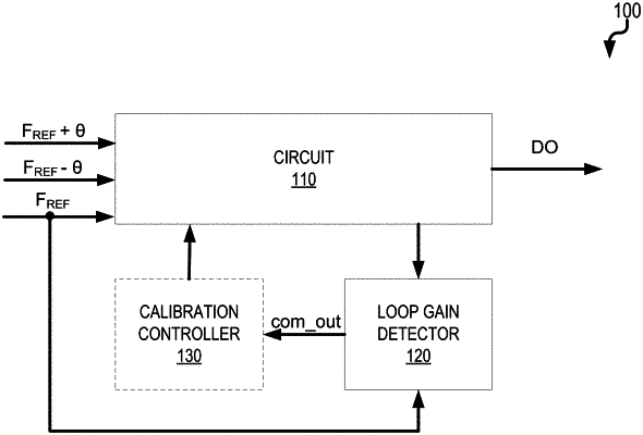
1. A device comprising:
a first phase detector circuit configured to detect a clock skew between a reference signal and an input signal;
a charge pump circuit configured to translate the clock skew into a voltage; and
a comparator configured to detect a loop gain associated with the input signal based on the voltage and output a loop gain signal for adjustment of the input signal.