| CPC H03K 17/6872 (2013.01) | 17 Claims |
|
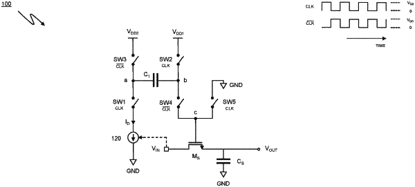
1. A sampling switch circuit, comprising:
an input node, connected to receive an input voltage signal to be sampled;
a sampling transistor comprising a gate terminal, a source terminal and a drain terminal, the source terminal connected to the input node;
a capacitor;
a current source configured to cause a defined current to flow therethrough; and
switching circuitry configured to alternate between a precharge configuration and an output configuration in dependence upon a clock signal,
wherein:
in the precharge configuration, the switching circuitry connects the capacitor into a current path between said current source and a first voltage reference node to form a potential difference across the capacitor which is dependent on the defined current; and
in the output configuration, the switching circuitry connects the capacitor between a second voltage reference node and the gate terminal of the sampling transistor so that a voltage level applied at the gate terminal of the sampling transistor is dependent on the defined current.
|