| CPC H03K 3/356104 (2013.01) [H03K 3/012 (2013.01); H03K 3/037 (2013.01)] | 3 Claims |
|
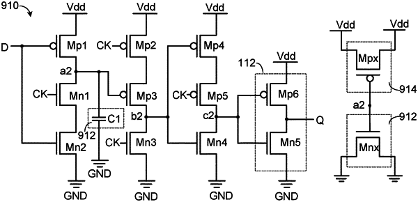
1. A D-type flip-flop, comprising:
a first first-type transistor having a gate terminal, a first drain/source terminal, and a second drain/source terminal, wherein the gate terminal of the first first-type transistor receives an input signal, the first drain/source terminal of the first first-type transistor receives a first supply voltage, and the second drain/source terminal of the first first-type transistor is connected to a first node;
a first second-type transistor having a gate terminal, a first drain/source terminal and a second drain/source terminal, wherein the gate terminal of the first second-type transistor receives a clock signal, and the first drain/source terminal of the first second-type transistor is connected to the first node;
a second second-type transistor having a gate terminal, a first drain/source terminal and a second drain/source terminal, wherein the gate terminal of the second second-type transistor receives the input signal, the first drain/source terminal of the second second-type transistor is connected with the second drain/source terminal of the first second-type transistor, and the second drain/source terminal of the second second-type transistor receives a second supply voltage;
a second first-type transistor having a gate terminal, a first drain/source terminal and a second drain/source terminal, wherein the gate terminal of the second first-type transistor receives the clock signal, and the first drain/source terminal of the second first-type transistor receives the first supply voltage;
a third first-type transistor having a gate terminal, a first drain/source terminal and a second drain/source terminal, wherein the gate terminal of the third first-type transistor is connected to the first node, the first drain/source terminal of the third first-type transistor is connected with the second drain/source terminal of the second first-type transistor, and the second drain/source terminal of the third first-type transistor is connected to a second node;
a third second-type transistor having a gate terminal, a first drain/source terminal and a second drain/source terminal, wherein the gate terminal of the third second-type transistor receives the clock signal, the first drain/source terminal of the third second-type transistor is connected to the second node, and the second drain/source terminal of the third second-type transistor receives the second supply voltage;
a fourth first-type transistor having a gate terminal, a first drain/source terminal and a second drain/source terminal, wherein the gate terminal of the fourth first-type transistor is connected to the second node, and the first drain/source terminal of the fourth first-type transistor receives the first supply voltage;
a fifth first-type transistor having a gate terminal, a first drain/source terminal and a second drain/source terminal, wherein the gate terminal of the fifth first-type transistor receives the clock signal, the first drain/source terminal of the fifth first-type transistor is connected with the second drain/source terminal of the fourth first-type transistor, and the second drain/source terminal of the fifth first-type transistor is connected to a third node;
a fourth second-type transistor having a gate terminal, a first drain/source terminal and a second drain/source terminal, wherein the gate terminal of the fourth second-type transistor is connected to the second node, the first drain/source terminal of the fourth second-type transistor is connected to the third node, and the second drain/source terminal of the fourth second-type transistor receives the second supply voltage;
a first capacitor comprising a fifth second-type transistor; and
a second capacitor comprising a sixth first-type transistor;
wherein a gate terminal of the fifth second-type transistor is connected to the first node, and a first drain/source terminal of the fifth second-type transistor and a second drain/source terminal of the fifth second-type transistor receive the second supply voltage, wherein a gate terminal of the sixth first-type transistor is connected to the first node, and a first drain/source terminal of the sixth first-type transistor and a second drain/source terminal of the sixth first-type transistor receive the first supply voltage.
|