| CPC H02M 3/158 (2013.01) [H02M 1/00 (2013.01); H02M 3/157 (2013.01); H02M 1/0016 (2021.05); H04R 3/00 (2013.01)] | 20 Claims |
|
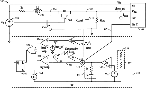
1. A power supply circuit comprising:
a boost converter comprising:
an inductive element coupled between an input voltage node and a switching node;
a first switch coupled between the switching node and a reference potential node; and
a second switch or a diode coupled between the switching node and an output voltage node; and
a feedback control circuit having a first input coupled to the output voltage node, having a second input configured to sense a current through the first switch, and having an output coupled to at least a control input of the first switch, the feedback control circuit comprising:
a voltage node configured to influence a duty cycle of the boost converter;
a feedforward path coupled to the voltage node and configured to have a voltage signal derived from an input voltage at the input voltage node;
a combiner having an output coupled to the voltage node and having a first input coupled to the feedforward path, such that the feedforward path is coupled to the voltage node via the combiner; and
a first comparator having a first input coupled to the second input of the feedback control circuit and having a second input coupled to the output of the combiner.
|