| CPC H02M 1/0095 (2021.05) [H02M 3/07 (2013.01); H02M 7/4837 (2021.05)] | 17 Claims |
|
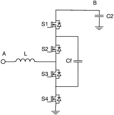
1. An inductive flying capacitor power converter comprising:
first, second, third, and fourth series-connected switches forming a switch ladder, wherein the first and fourth switches are operated as a first complementary switch pair and the second and third switches are operated as a second complementary switch pair;
an inductor having a first inductor terminal coupled to a converter terminal and a second inductor terminal coupled to a junction between the second and third switches; and
a flying capacitor having a first flying capacitor terminal coupled to a junction of the first and second switches, a second flying capacitor terminal coupled to a junction of the third and fourth switching devices, and a flying capacitor voltage between the first and second flying capacitor terminals;
a control circuit that generates a first pair of complementary gate drive signals to drive one of the first or second complementary switch pairs and a second pair of complementary gate drive signals to drive the other of the first or second complementary switch pair, wherein the control circuit varies a phase shift between the first pair of complementary gate drive signals and the second pair of complementary gate drive signals to regulate the flying capacitor voltage, wherein varying the phase shift between the first pair of complementary gate drive signals and the second pair of complementary gate drive signals shifts the timing of a charging window of the flying capacitor so that,
varying the phase shift in a first direction shifts timing of a charging window to cause an output charge from the flying capacitor to exceed an input charge to the flying capacitor, thereby decreasing the flying capacitor voltage; or
varying the phase shift in a second direction shifts timing of a charging window in a second direction to cause an input charge to the flying capacitor to exceed an output charge from the flying capacitor, thereby increasing the flying capacitor voltage.
|