| CPC H01Q 1/273 (2013.01) [G04G 21/02 (2013.01); G04G 21/025 (2013.01); G04G 21/04 (2013.01); G04R 60/06 (2013.01); G04R 60/12 (2013.01); H01Q 1/24 (2013.01); H01Q 1/243 (2013.01); H01Q 1/27 (2013.01); H01Q 3/24 (2013.01); H01Q 9/04 (2013.01); H01Q 9/0464 (2013.01); H01Q 9/42 (2013.01); H01Q 5/378 (2015.01); H01Q 7/00 (2013.01)] | 20 Claims |
|
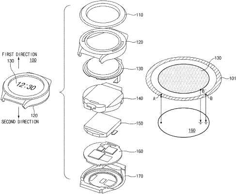
1. A wearable electronic device comprising:
a housing comprising a metal structure;
a display positioned within the housing, the display including a metal layer positioned within the metal structure and at least partially spaced apart from the metal structure;
a printed circuit board (PCB) positioned within the housing and including a ground region and a control circuit configured to feed a first point of the metal structure; and
at least one first conductive connection member comprising a conductive material, the at least one first conductive connection member electrically connected with a third point of the metal structure;
wherein the metal layer is electrically connected with the ground region of the PCB at a second point spaced apart from the first point,
wherein the at least one first conductive connection member is electrically coupled to the ground region of the PCB.
|